Jonas Energy
1 / 5
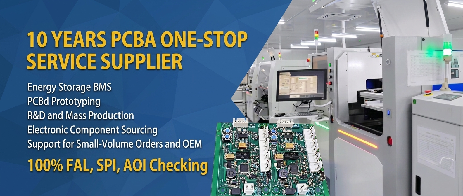

| SMT Technical Specifications | |
|---|---|
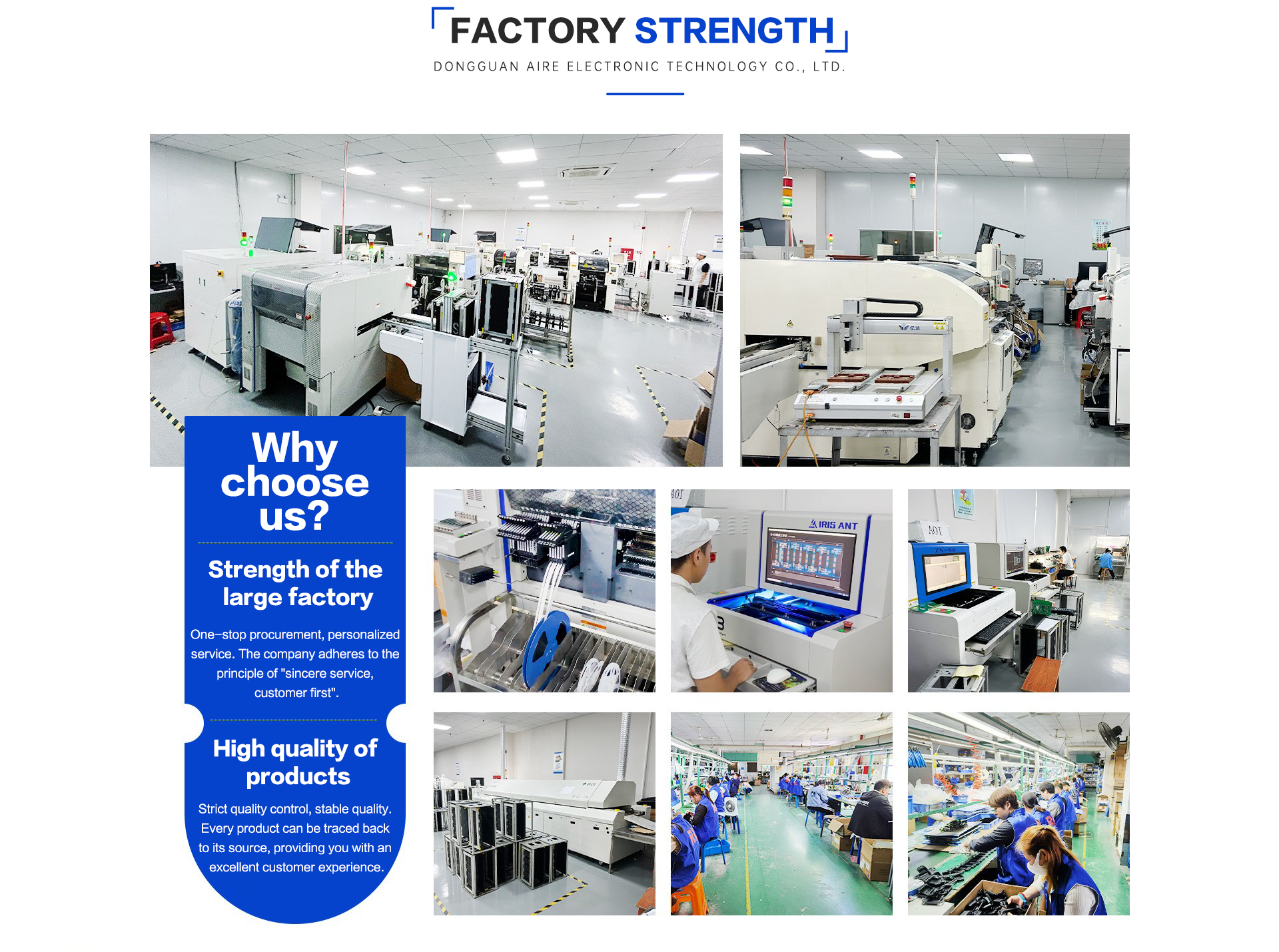
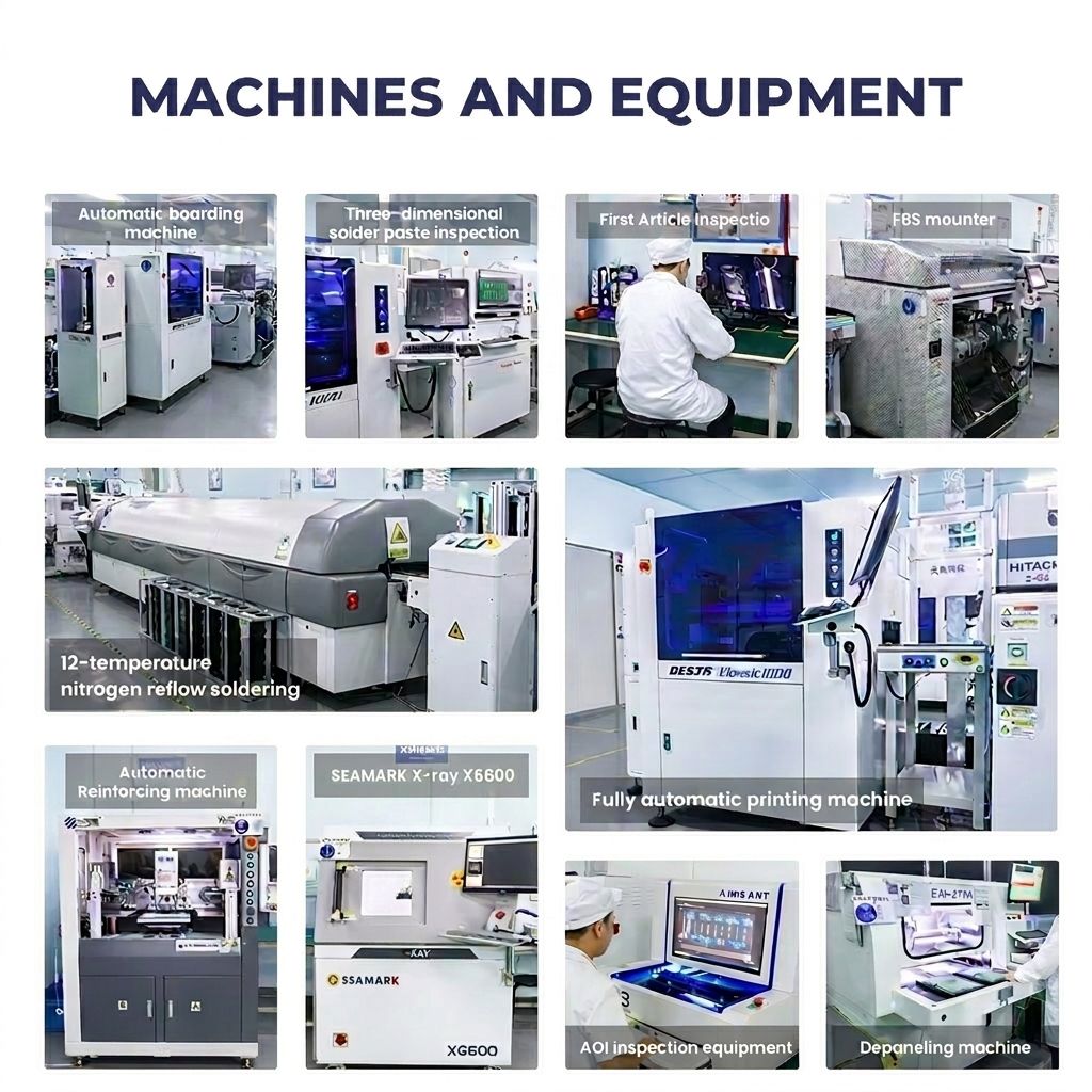
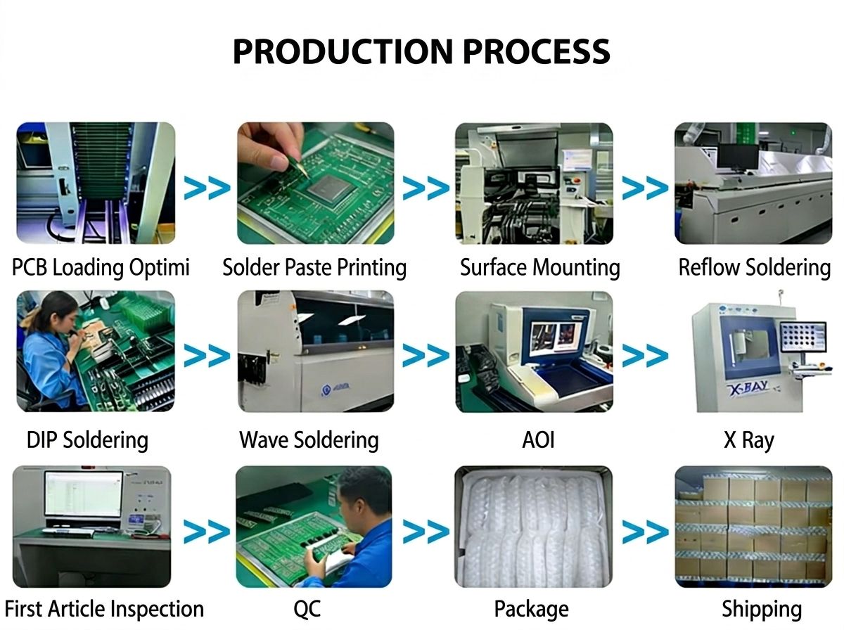
| Solder Paste Printing Accuracy | ±0.025 mm |
| Max Solder Paste Printing Speed | 150 mm/s |
| Solder Paste Printing | PCB Thickness: 0.2–6 mm |
| SMT Accuracy | ±0.05 mm |
| SMT Speed | 0.048 sec/component |
| Max SMT PCB Size | 400 * 510 mm |
| Min SMD Resistor & Capacitor Size | 0201 |
| Min BGA R-VTx Pitch | 0.35 mm |
| Reflow Soldering Temperature Accuracy | ±4°C |
| Reflow Soldering Zones | 8 |
| Reflow Soldering | Lead-free |
| AOI Accuracy | ±0.0024 mm |
| AOI Speed | 5 in²/s (60 FOV/s) |
| AOI Capable Components | 0201 Chips & Fine Pitch |
| X-ray Inspection | BGA Voids (0.35 mm Pitch) |
| BGA Rework Station | Capable |
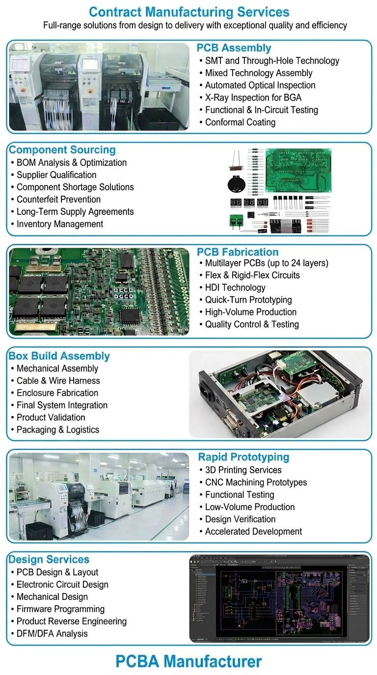
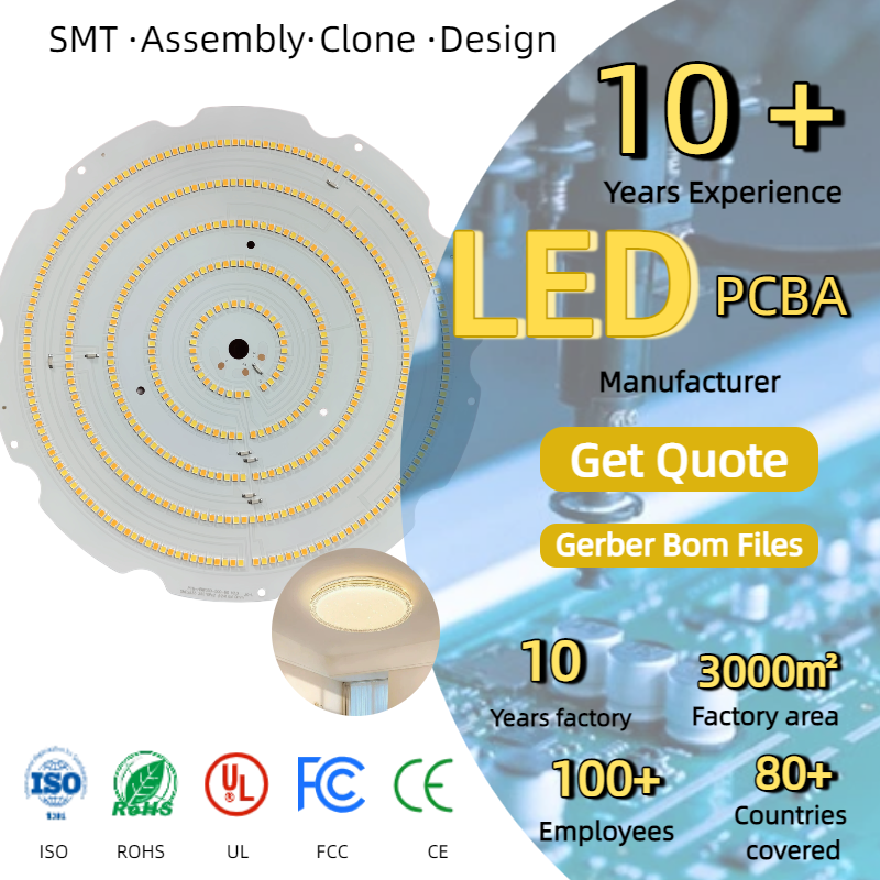
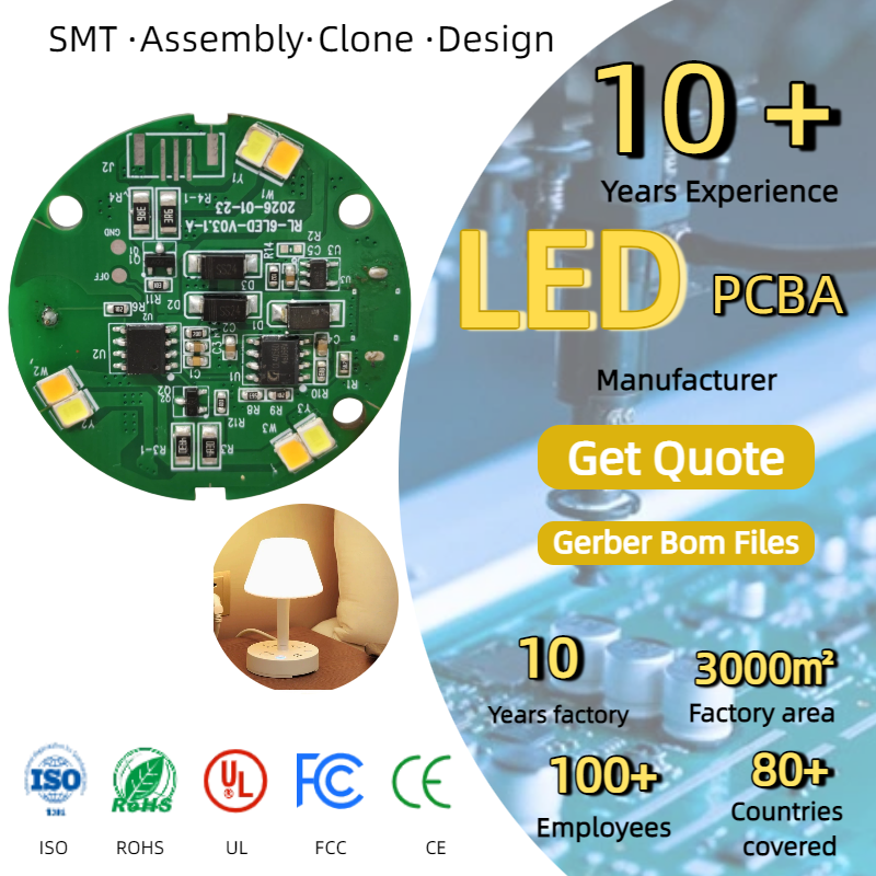
| PCB Technical Specifications | |
|---|---|
| Layers | 1–40 layers |
| Base Material | FR4, High-TG FR4, CEM3, aluminum, High Frequency (Rogers, Taconic, ArOn, PTFE.F4B) |
| Max Panel Size | 1200*400mm |
| Min Board Thickness |
4 layers: 0.40 mm 6 layers: 0.80 mm 8 layers: 1.00 mm 10 layers: 1.20 mm |
| Min Line Width/Spacing | 0.065 mm |
| Min Line Spacing to PSD | 0.09 mm |
| Min Line Width Tolerance | +/- 10% |
| Min Finished Hole Size | 0.10 mm |
| Hole Wall Copper Thickness | Max 35 µm |
| Max Copper Thickness in Pattern | 210 µm |
| PTH Hole Diameter Tolerance | 0.05 mm |
| NPTH Hole Diameter Tolerance | 0.025 mm |
| Aspect Ratio | 10:01:00 |
| Hole Position Accuracy | Min +/- 0.05 mm |
| Copper weight | 0.5-6oz |
| Acceptable File Format | Gerber file, PowerPCB, CAD, AUTOCAD, ORCAD, P-CAD, CAM-350, CAM2000 |
| Certificate | ROHS, ISO9001, CE, FCC |

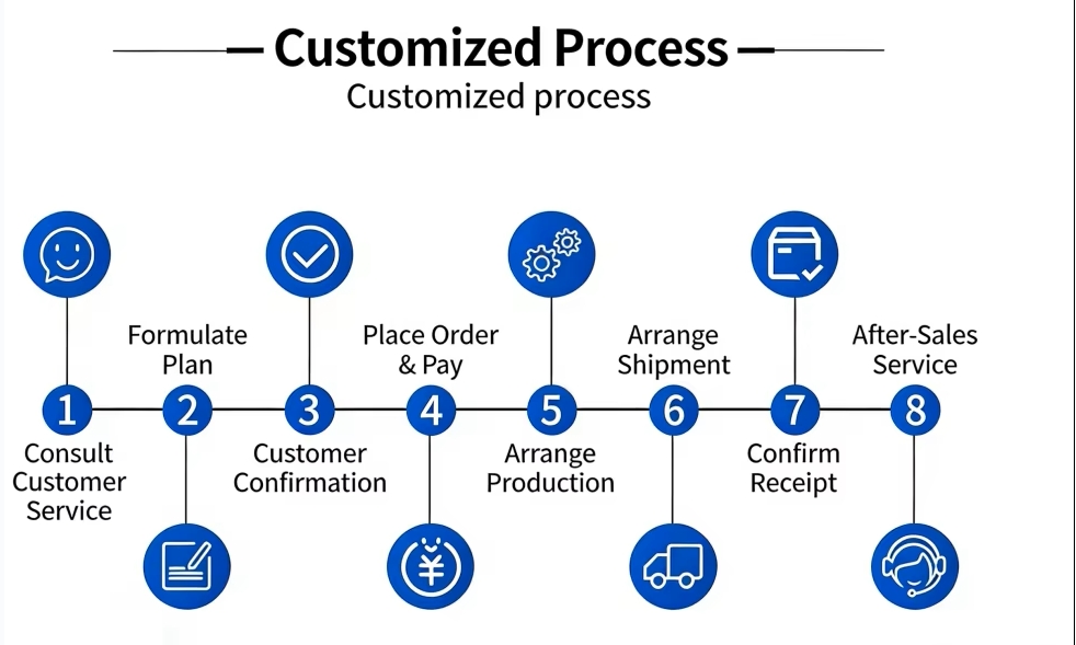

Ready to bring your project to life? Click "Get Quote" or "Chat Now" to talk to our engineering team. We support OEM/ODM customization to meet your specific needs!


| Item | Description |
|---|---|
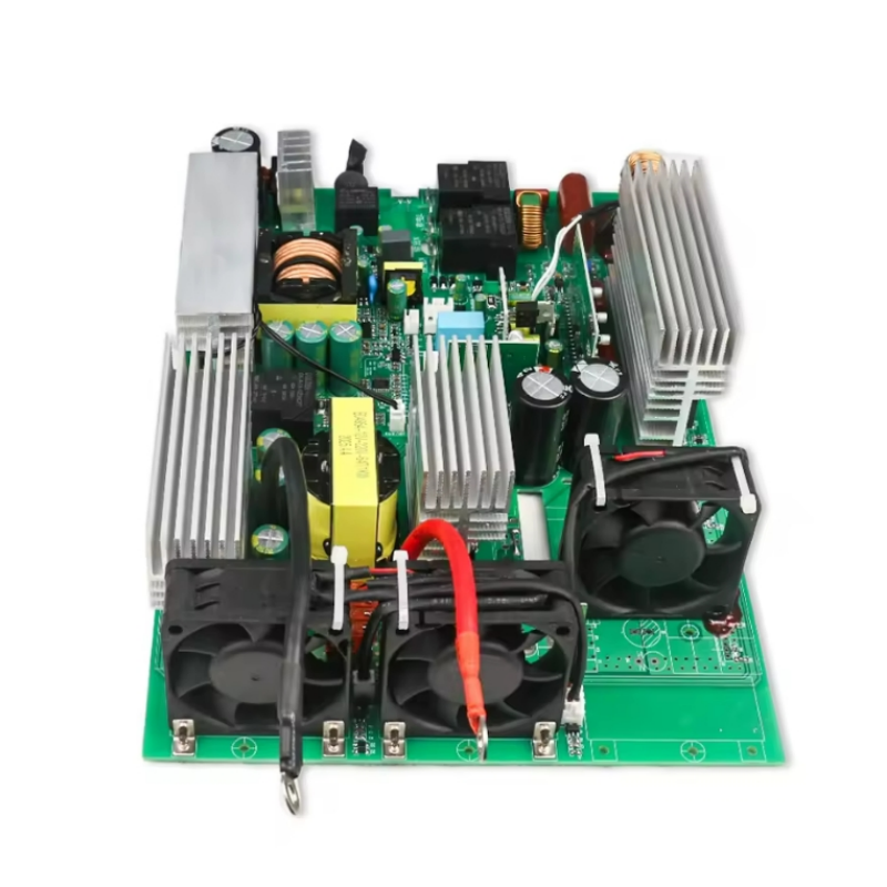
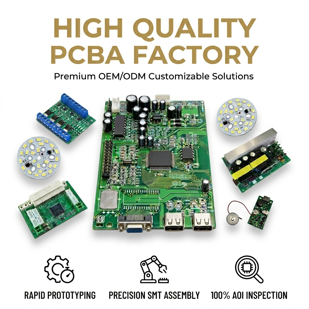
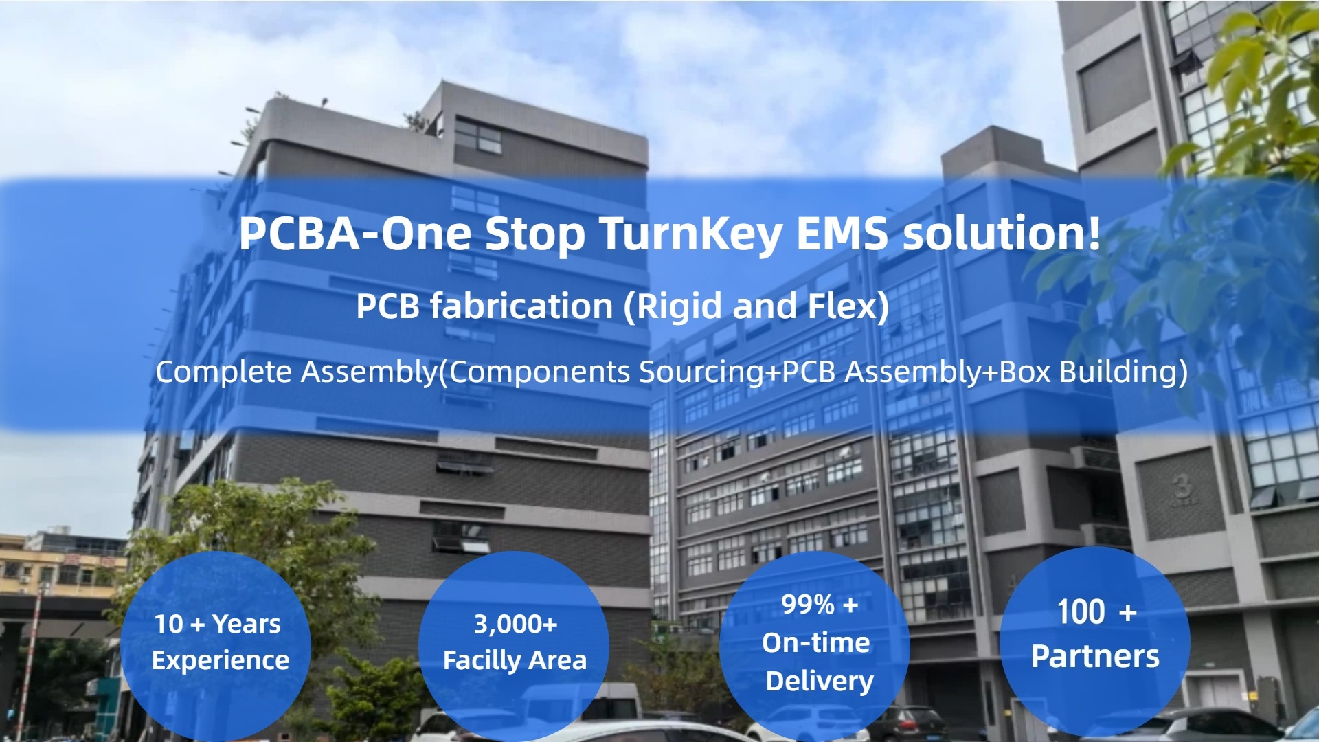
| Product Range & Services | PCB manufacturing, PCBA assembly (SMT/DIP/THT), turnkey PCBA, OEM/ODM. PCB types: single/double/multilayer/HDI/rigid/flex/rigid-flex/aluminum/LED. Services: prototype, small batch, mass production, quick-turn fabrication & assembly. |
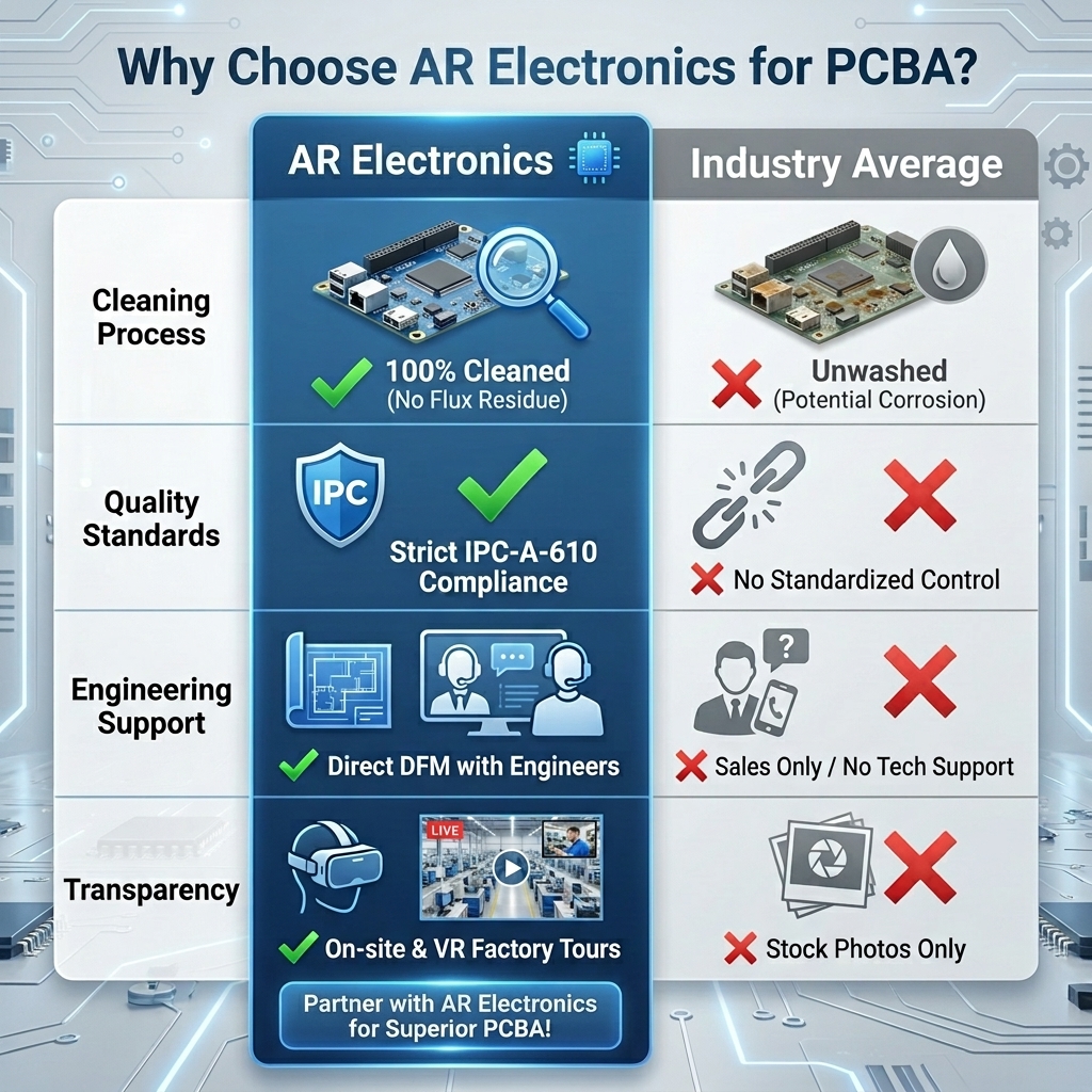
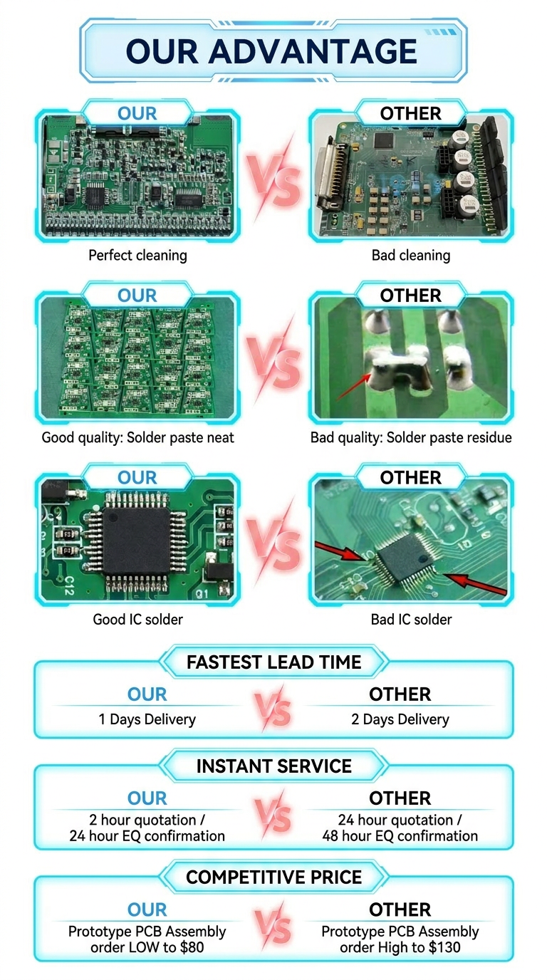
| Quality Control Process | Full QC: incoming material (CCL, solder mask, components), in-process, AOI, X-ray (BGA/QFN), ICT/flying probe, functional, final inspection. IPC-A-600/610 standards, traceable records, strict AQL. Low defect rate, stable quality. |
| Electrical & Functional Testing | 100% E-test (open/short), impedance test for high-speed. PCBA functional test, ICT, flying probe, aging, temp/humidity reliability on request. Critical PCBA individually powered & tested before shipment. |
| Materials & Technologies | PCB materials: FR4, high-TG, halogen-free, RF/high-freq, aluminum base. Surface finishes: HASL LF, ENIG, OSP, immersion tin/silver, hard gold. Technologies: fine-pitch SMT, BGA, QFN, COB, 0201/01005, mixed assembly, conformal coating, potting, box build. |
| Engineering & DFM Support | Professional CAM/engineering, free DFM review (Gerber, BOM, PnP). Support stack-up, impedance, panelization, stencil, component substitution, BOM optimization. One-stop from layout to fabrication & assembly. |
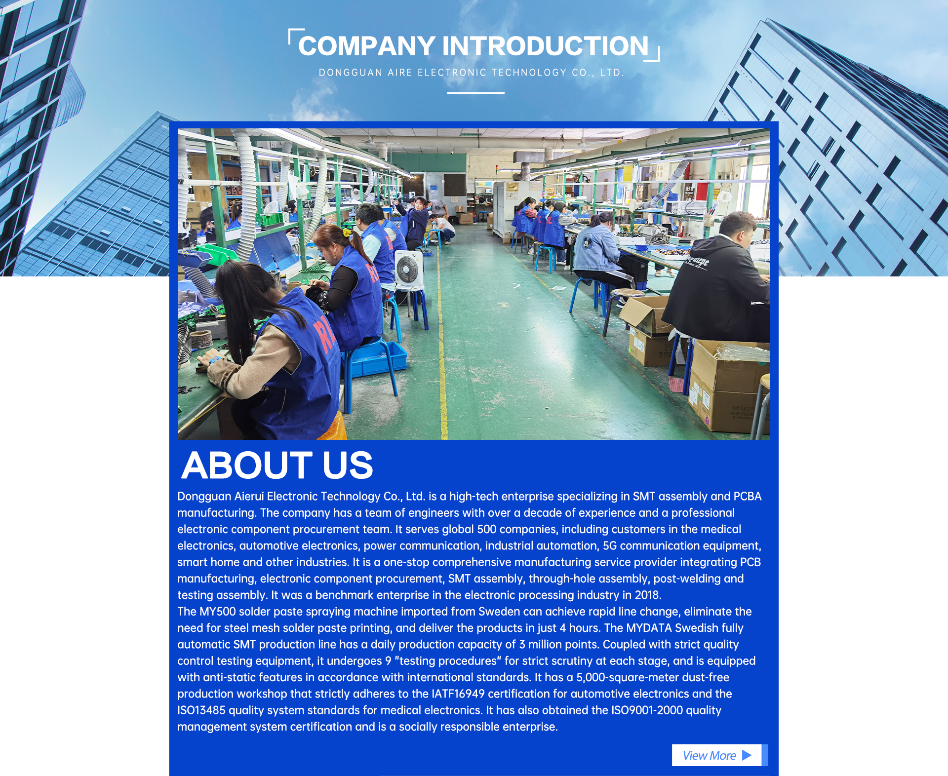
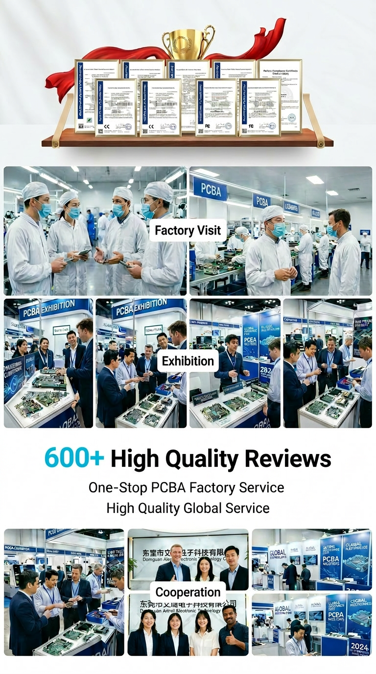
| Certifications & Compliance | Production compliant with ISO9001, ISO14001, IATF16949, UL, RoHS, REACH. |
| Production Capacity & Lead Time | Stable capacity for prototype to mass production orders. |
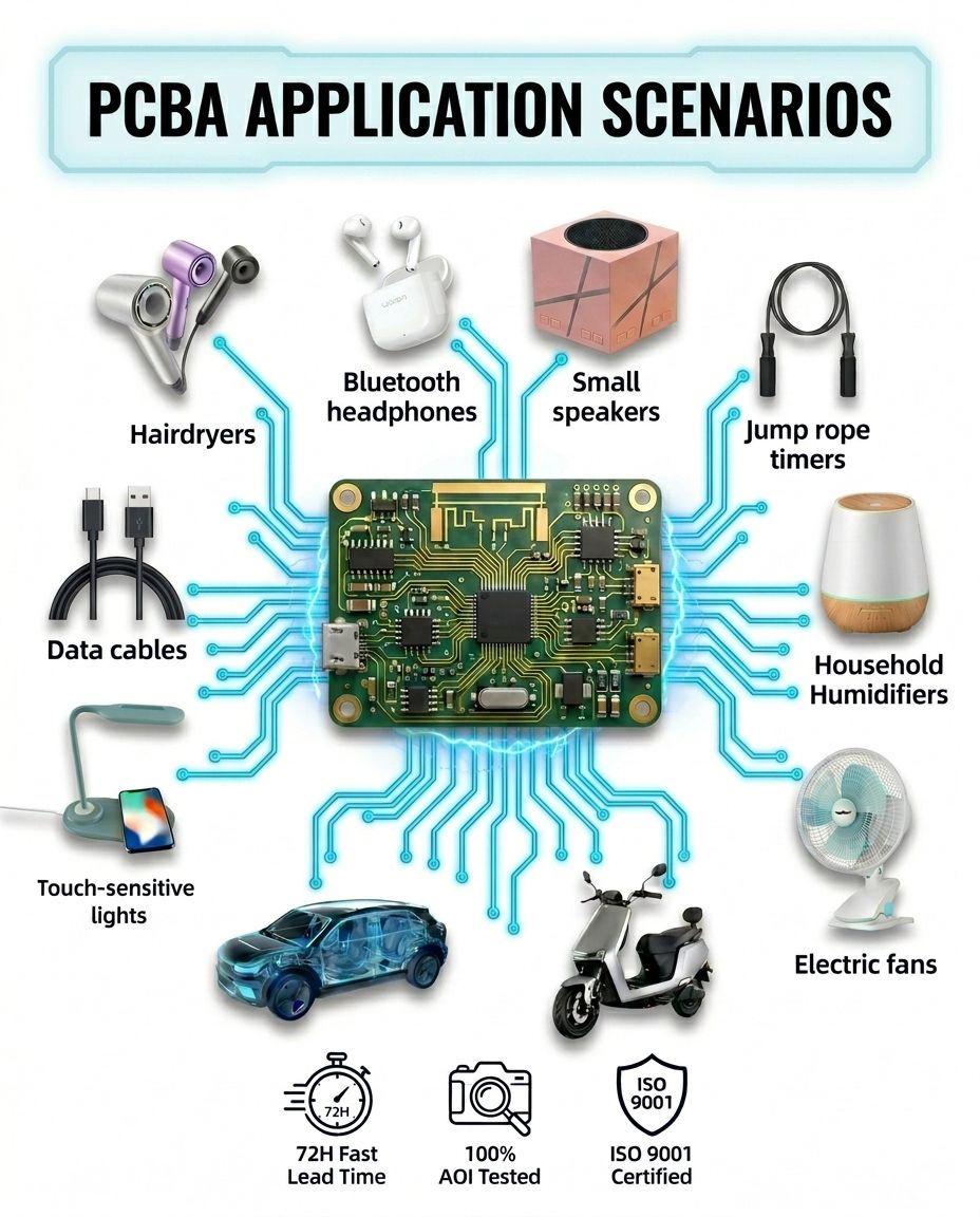
| Industries & Application Fields | Industries served: consumer electronics, industrial control, power, communication, automotive, medical, smart home, IoT, LED lighting, security, new energy, etc. High-quality PCBs/PCBAs. |
| Warranty & After-Sales Service | Warranty on manufacturing defects. Rework/replace/refund per inspection report; fast response. English-speaking support, quick feedback & technical analysis. |
| Online Reputation & Advantages | Alibaba Verified, Trade Assurance, on-time delivery, secure payment. Global customers (Europe, N.America, Asia). One-stop: PCB fab, component sourcing, SMT/DIP, testing, packaging in one factory. |
Contact us today about your PCBA project, and our professional engineers will provide you with personalized solutions.